Industry summary
Semiconductor industry has the characteristics of large exhaust volume and low emission concentration. Volatile organic waste gas mainly comes from the processes of lithography, development, etching and diffusion. In these processes, the wafer surface should be cleaned with organic solution (such as isopropanol), and the volatile waste gas is one of the sources of organic waste gas. At the same time, the photoresist (photoresist) used in the process of lithography and etching contains volatile organic solvents, such as butyl acetate Wafer processing also volatilizes into the atmosphere, which is another source of organic waste gas. There are a lot of organic compounds in the cleaning agent, developer, photoresist, etching solution and other solvents used in semiconductor manufacturing process. In the process, most of these organic solvents are volatilized into exhaust gas.
Industry solutions
At present, the treatment of organic waste gas emission adopts large air volume and low concentration, and the treatment generally adopts the combination of adsorption concentration and incineration, with the treatment efficiency of more than 95%.
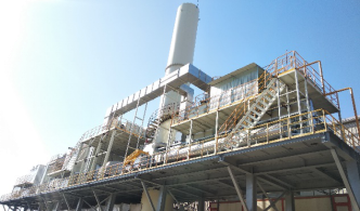
Case 1:A well-known U.S. mobile phone glass company adopts Huashijie All in One Machine with ZCR.
Molecular sieve runner + thermal oxidation • Regenerative thermal oxidation RTO • Adsorption recovery
Customer served

- • VOCs adsorption and concentration treatment
- • Thermal oxidation/catalytic oxidation
- • Adsorption and recovery of high concentration VOCs
- • Biological treatment of odor VOCs
- • Industrial dust and oil mist filtration
- • Heat recovery
- • Dehumidification
- • Indoor purification
- • VOCs Online Monitoring Platform

 Nationwide service line:400 0377 123


